Optics – Materials for microoptics, photonics and optoelectronics

In opto-electronics and the optical industry, micro-optical components, such as lenses, gratings, photonic crystals or diffractive optical elements, are used to an increasing degree in environments that require high stability to aging. Whether for high volume production or for the manufacturing of highly specific individual components, it is essential to reduce production costs and materials consumption.

Compared to purely polymeric materials, inorganic-organic hybrid polymers have excellent optical properties plus the potential to be adapted to given requirements owing to their chemical structure and versatile processing options. A number of structuring methods is available, but the nano-imprint lithography and the 2-photon polymerization (2PP) are especially suited to realize complex three-dimensional forms. Moreover, the materials are compatible with microelectronic and common semiconductor production processes.


R&D priorities

The uncoupling and coupling of light plays a central role in efforts to increase the efficiency of LEDs, OLEDs, solar cells and displays. Depending on given requirements, the Fraunhofer ISC develops purely inorganic or hybrid layers with specific refractive indexes, scattering properties or surface roughness and structures to improve the performance of the elements.


Methods and technologies

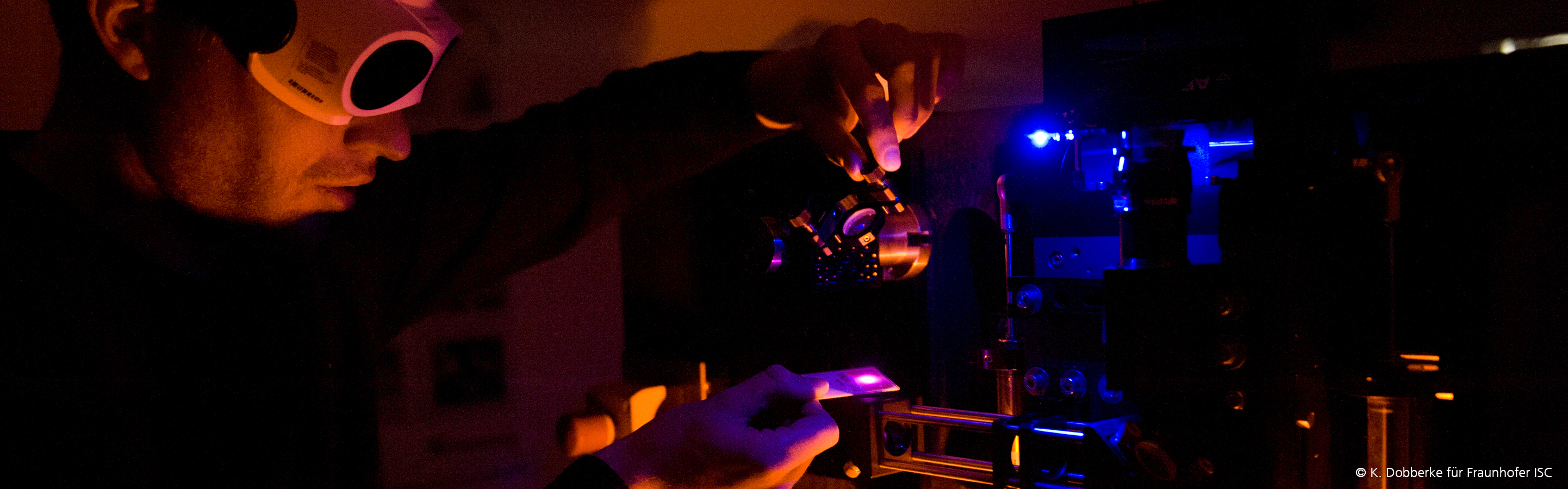
Optical data transmission is more and more important in information and communication technology. This is due to ever larger data volumes and involved thermal and electrical challenges resulting from the continuous miniaturization along with increased integration density. Waveguide materials, which can be used for single or multimode waveguides with as little loss as possible both in terms of their production as of their intrinsic properties, play a key role in this context.

Fraunhofer ISC technologies seek to optimize the spatial design of the waveguides and the coupling/uncoupling of opto-electronic components, in particular in optical packaging solutions for boards, modules and chips. The two-photon polymerization developed for these purposes by the Fraunhofer ISC allows for the energy- and resource-efficient production of three-dimensional optical waveguides and is compatible with customary assembly processes.

Video: project Go Beyond 4.0

Source: Youtube

Privacy warning

With the click on the play button an external video from www.youtube.com is loaded and started. Your data is possible transferred and stored to third party. Do not start the video if you disagree. Find more about the youtube privacy statement under the following link: https://policies.google.com/privacy

Individual component manufacturing in mass production

Within the project “Go Beyond 4.0”, six Fraunhofer institutes have succeeded in using digital printing and laser processes to individually integrate, for example conductor tracks and sensors into components. The need for individualized components with sophisticated functionalities in industrial mass production is growing. With digital printing and laser technologies, the new challenges can be easily mastered in the future.

An ink consisting of an optical hybrid polymer, the so-called ORMOCER®, is used to create individualized optics. The material developed by Fraunhofer ISC has outstanding optical properties similar to good optical glasses and can be specifically adapted to the respective application.


Whitepaper:
Compatibility of ZrO2 Nanocrystals

In a variety of applications, non-yellowing, easy-processable bulk materials with high refractive indices (> 1.6) are needed in order to improve performance and/or efficiency of optical and electro-optical devices and components. Facing these demands, most common approach is the use of composite material consisting of a polymeric matrix and high-refractive nanoparticles.  


Two-Photon
Polymerization

Many applications in everyday life as well as in laboratory environment are enabled by highly miniaturized and specially designed devices. Particularly the field of micro-optics in e.g. micro-imaging, beam-shaping and integrated optics is a crucial factor for increased performance and further miniaturization of devices and setups. Aspheric and freeform surfaces might further advance the application of micro-optics in optical system.


Fraunhofer Lighthouse Project Go Beyond 4.0

Individualization of Products in Mass Production: Development of cutting-edge Technology within the Fraunhofer Lighthouse Project »Go Beyond 4.0«

Your local contact

Gerhard Domann

Contact Press / Media

Gerhard Domann

Head of CeSMA

Fraunhofer Institute for Silicate Research ISC
Neunerplatz 2
97082 Würzburg, Germany

Phone +49 931 4100-551